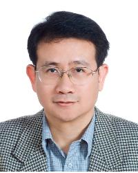
林清富 Ching-Fuh Lin
Founding Director of Innovative Photonics Research Center
主要研究領域:
太陽能無人機、太陽能電池及光電元件、單晶矽薄膜太陽能電池與矽奈米線太陽能電池、氧化鋅發光二極體、矽光子、寬頻半導體雷射以及半導體光放大器。Major Research Areas:
Organic-inorganic composite thin-film solar cells 、Single-crystal Si thin-film solar cells & 、ZnO-based LEDs 、Si-based photonics 、Broadband semiconductor lasers and optical研究領域摘要:
Research Summary:
(一) 英文
l Explore organic solar cells with inverted structures. The organic layer is sandwiched by two oxides to provide good protection on the organic materials for improved stability and electron/hole blocking functions for efficient cerrier collection. The most promising part of this technique is that the sandwiched structure is fabricated using full solution process, so the cost could be very low and the production is potentially high for its compatibility with printing technology. Also, technology of forming very thin film of crystalline Si is developed.
1. Develop Si nanowires/PEDOT solar cells with efficiency >10%.
2. Invent solution processing technology for sandwiched inverted structures of ZnO /organic photovoltaic devices to achieve power-conversion efficiency of above 7 %.
3. Achieve good stability of unencapsulated organic solar cells with the efficiency retained 95% of the best vaue after 14500 hours of the fabrication.
4. Invent massive transfer technology of vertically aligned nanowires/nano-structure film from crystalline wafer.
5. Invent massive transfer technology of crystalline Si thin film to alien substrates to alien substrates to enable Si-soalr cells with very low material cost.
(二) 英文
l Investigation on the influences of nano-structures on photonics. The confinement of electron-hole pairs in the nano-domain gives rise to very different behaviors in the Si crystals, leading to greatly enhanced radiative-recombination probability. Also, the nano-structures in organic-inorganic composites result in significantly enhanced power conversion efficiency of photovoltaic devices. In this area, we have achieved the following results
1. First demonstration of nearly lasing phenomena such as threshold behavior and resonance modes from Si at the Si bandgap energy with the assistance of SiO2 nanoparticles. (News report by MRS Bulletin News, June 2002 and NewsBreaks in Laser Focus World, March 2003).
2. Achieve external quantum efficiency > 10-4 at the Si bandgap energy from metal-SiO2 nanoparticle-silicon structure on Si.
3. First demonstration on the modification of the black-body radiation to significantly enhance the blue spectrum using metallic photonic boxes based on Si fabrication technology.
4. Invent laser reformation technique to smoothen the surface of Si waveguides and sub-micro-sphere resonators with surface roughness reduced to less than 0.2 nm.
(三) 英文
l Research on carrier distribution and dynamics in non-identical quantum wells and quantum dots for broadband semiconductor optical devices. The carrier distribution in non-identical quantum wells is not uniform, but can be engineered, so broadband characteristics can be realized by proper layout of the quantum-well structure. With our investigation, we are able to achieve the following record research results.
1. Achieve record broadband superluminescent diodes, FWHM bandwidth: 400 nm (1250- 1650nm) for InGaAsP/InP type and 91.5 nm (763 ~ 854.5 nm) for AlGaAs/GaAs type.
2. Achieve record tuning range for tunable semiconductor lasers, single wavelength tuning range 240 nm (from 1300 nm to 1540 nm).
3. Achieve record tuning range for tunable dual-wavelength semiconductor lasers with spectral separation tunable from a few nm up to 190 nm.
4. Simultaneous generation of 8 channels with 20 nm channel spacing, spanning from 1367 nm to 1527 nm.
5. Discover new factors that influence the nonuniform carrier distribution among multiple quantum wells.

-
B.S.
Electrical Engineering, National Taiwan University, 1983 -
M.S.
Electrical Engineering, Cornell University , 1989 -
Ph.D.
Electrical Engineering, Cornell University, 1993
-
Address
BL-414,
Department of Electrical Engineering,
National Taiwan University,
Taipei 106, Taiwan -
Phone
+886-2-33663540 -
FAX
+886-2-2364 2603 -
Email:

-
Office Hour
Mon. 2:30-3:30 pm, Wed. 2:00-3:00 pm.