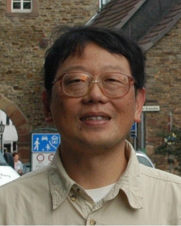
林浩雄 Hao-Hsiung Lin
主要研究領域:
化合物半導體材料與元件, 分子束磊晶技術Major Research Areas:
Compound semiconductor materials and devices based on molecular beam epitaxy研究領域摘要:
主要的研究領域為三五族化合物半導體分子束磊晶技術與相關的光電元件技術。研究過的材料包括AlGaAs / GaAs、InGaAs / GaAs、InGaAsP / InP、含氮與含銻化合物半導體合金塊材、量子井與量子點結構。元件則包括異質接面雙極性電晶體與雷射二極體等。目前進行的研究包括:
(1) 低含氮化合物半導體(Diluted nitrides):
在傳統半導體材料摻氮的低含氮半導體,因為氮的加入造成晶格與能隙的同時縮減。這個特點可以拓展化合物半導體的領域,但是摻氮也帶來了許多材料上值得研究的課題。我們過去曾從事InAsN含氮材料的研究,成長InAsN/InGaAs量子井並達到2.4 mm的雷射震盪。目前主要成長與GaAs晶格匹配但能隙低於1-eV的低含氮GaAsSbN。應用為高效率solar cell與HBT。
(2) 中紅外線(Mid-infrared, MIR)化合物半導體:
MIR是許多化學氣體、液體、生物分子的吸收特徵波段。我們與英國Lancaster Univeristy合作以GSMBE(氣態源分子束磊晶法)成長適用於3-5 mm的InAsPSb四元材料以及InAsPSb/InAsSb量子井結構,並應用此結構來製作光電元件。
(3) 奈米結構的異質磊晶技術:
在矽與氧化物所構成的奈米結構中,使用分子束磊晶技術填入三五族材料。研究三五族與矽的異質磊晶,以及選擇性磊晶的技術。可以應用到未來的積體電路。
Research Summary:
Our research field is mainly on the materials and devices of III-V compound semiconductor based on molecular-beam epitaxy (MBE) technology. Our first research project is the growth and characterization of dilute nitrides including GaAsSbN and InAsN. We have wide experiences on both materials. In 2002, we first demonstrated a 2.4 microns InAsN quantum well laser which possesses the longest wavelength among nitride lasers. We also have demonstrated GaAsSbN lattice-matched to GaAs and with a narrow energy gap of 0.8 eV.
Our second project is the growth and characterization of InAsPSb alloy. We are the first group to deposit this alloy using gas-source MBE. In this subject, we have a long collaboration work with Prof. Krier at Lancaster University (UK) since 2003. Recently, we worked on the determination of the electronic structure of ternary InAsSb, including the spin-oribit, fundamental gap and band offset. For details, please refer to our publication list.
Our third project is the heteroepitaxy of III-V compounds on patterned Si, which is supported by TSMC. The purpose is to explore the feasibility of replace the Si channel with III-V alloy.

-
B.S.
National Taiwan University, 1978 -
M.S.
National Taiwan University, 1980 -
Ph.D.
National Taiwan University, 1985
-
Address
EE2-419,
Department of Electrical Engineering,
National Taiwan University,
Taipei 106, Taiwan -
Phone
+886-2-33663670 -
FAX
+886-2-23671909/2363 -
Email:

-
Office Hour
Thursday PM5:30~6:30, Friday AM8:00~9:00