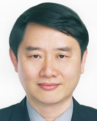
胡振國 Jenn-Gwo Hwu
國立台灣大學電子工程學研究所教授
Professor, Graduate Institute of Electronics Enginering, National Taiwan University
主要研究領域:
矽金氧半元件/超薄閘極氧化層製程技術/新型矽基元件/快速熱機台及製程/均勻度分析及應力控制/矽金氧半太陽電池及光感應器Major Research Areas:
Si MOS Devices/Ultra-thin Gate Oxide Processes/Novel Si-based Devices/Rapid Thermal Processing-RTP /Uniformity Analysis and Stress Control/Si MOS Solar Cell and Photo Sensors研究領域摘要:
主要研究方向為矽基材料上之金氧半(MOS)元件,尤其是有關超薄閘極絕緣層之研發。
利用純水中加上電場技術,將超薄SiO2 (< 2.5 nm)不均勻處予以自動補償,使電特性改善,漏流降低;利用超薄金屬鋁之液相氧化,經由電場及時間之準確控制,可使氧化膜形成高介電係數氧化鋁,同時在界面形成適當之SiO2層,達到低成本高品質之新型高介電係數閘極絕緣層開發;利用超薄氧化層MOS(p)元件於正偏壓下電流飽和之特性,製作溫度感測器,可整合於先進IC製程,監控電路溫度變化,靈敏度可達近2V/oC;利用超薄氧化層MOS(p)元件於正偏壓下電流飽和之特性,作為晶格表面受到應力施加情形之感測,得知晶圓之應力分布,及元件受應力之衰退機制;利用快速熱(RTP)及流場之控制,可得不同熱應力下之元件特性,提供有效之應力研究環境,並改善應力均勻度;在RTP中晶圓承接台及上方加上不同之材料,可得較佳之溫度分布;利用自製之重覆脈衝加熱(RSO)技術,可得較佳之超薄氧化層後厚度均勻度;利用H2SiF6溶液於電場下快速成長室溫氧化層,可得低成本MOS太陽電池,效率可達10 %;利用MOS元件之C-V深空乏特性,分析不均勻分布;利用邊緣高電場效應,製作高靈敏光偵測器;利用MOS之I-V微分特性,分析超薄氧化層厚度及不均勻分布;利用雙MIS穿隧二極體耦合特性製作類電晶體及記憶體。
研究以實作為主,結合精準之I-V及C-V量測得知元件特性,經分析解釋得知原理並進行改善,進而研發新型元件,提供學術界及業界參考。
Research Summary:
The major research topics are on the Si Metal-Oxide- Semiconductor (MOS) devices, especially on the study of ultra-thin gate oxides.
Using the compensation of anions through ultra-thin oxides via the field stress in D.I. water, the oxide will become more uniform and less leaky. By suitably controlling anodization time and field, one can obtain cost effective high-k Al2O3 by the oxidation of thin Al film. Using the saturation characteristic of I-V curve of MOS(p) devices, one can detect the temperature and stress distribution within the wafer. By adding suitable susceptors and cover quartz on wafer, one can control the temperature and flow distribution in RTP, and therefore the uniformity of oxide thickness. Using anodization in H2SiF6 solution, one can prepare room temperature MOS solar cells with efficiency close to 10 %. Analysis of the lateral non-uniformity in MOS structure by examining the deep depletion behavior in C-V curves. High sensitive photo sensors by using the enhanced fringing field effect of MOS structure at edge. Determination of the thickness of ultra-thin oxide and examining the non-uniformity property in it by analyzing the derivative of the I-V curve of MOS structure. Transistor and memory devices by utilizing the coupling effect in concentric MIS tunneling diodes.
Experiments are essential in the study of devices. From measurements and analyses, devices’ characteristics are explained and novel devices are proposed.

-
B.S.
EE, National Chiao-Tung University, 1977 -
M.S.
EE, National Taiwan University, 1979 -
Ph.D.
EE, National Taiwan University, 1985
-
Address
EE2-446,
Department of Electrical Engineering,
National Taiwan University,
Taipei 106, Taiwan -
Phone
+886-2-33663646 -
FAX
+886-2-23671909 -
Email:

-
Office Hour
Monday and Wednesday PM.1:30 ~3 :00