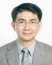
蔡坤諭 Kuen-Yu Tsai

Dr. Kuen-Yu Tsai was born in Taipei, Taiwan, in 1973. He received his B.Sc. degree in 1995 and his M.Sc. degree in 1997, both in mechanical engineering, from National Taiwan University. From 1995 to 1997, he was a Research Assistant of National Science Council (the predecessor of Ministry of Science and Technology), Taiwan, working on projects led by Prof. Jia-Yush Yen regarding ultra-precision wafer positioning problems in photolithography systems and an interferometer-limited resolution of 5 nm was achieved. From 1998 to 2002, he was a Ph.D. student in Department of Aeronautics and Astronautics, and a Research Assistant of Information Systems Laboratory in Department of Electrical Engineering, both at Stanford University. He received his Ph.D. degree in aeronautics and astronautics, with a minor in electrical engineering. He worked on DARPA and NSF projects aiming at applying multivariable control, simulation, optimization, and signal processing techniques to semiconductor manufacturing problems, a multidisciplinary research direction pioneered and led by Prof. Thomas Kailath (IEEE Medal of Honor, 2007) in the 1990s and early 2000s which turned out to be highly successful and influential to both the academia and the industry worldwide. He developed innovative control and signal processing algorithms targeting at nanoimprint-based next-generation lithography systems (partly under Prof. R. Fabian Pease's supervision), and obtained one US patent granted and the other pending. He closed his dissertation work under the guidance of Prof. Stephen P. Boyd (IEEE Control Systems Award, 2013).
From 2002 to 2005, Dr. Tsai was a Senior Process Engineer in lithography of Intel Corporation. At Intel he worked on performance monitoring and improvement of 193-nm microlithography scanners at Fab-D1C in Hillsboro, Oregon, and Fab-11X in Rio Rancho, New Mexico, for Intel's P1262 90-nm process technology with then-just-introduced 300-mm wafer facilities. He also conducted research projects under the supervision of Dr. Alan R. Stivers in the Advanced Mask Technology group of Components Research in Santa Clara, California, on defect inspection specifications and inspection tool development for EUV lithography then targeted for the ITRS 32 nm half-pitch node (aka "16/14 nm node") and beyond.
Since 2005, Dr. Tsai has joined the faculty of National Taiwan University, starting as an Assistant Professor in Department of Electrical Engineering. He has founded and served as the directors of Nanoscale Design and Fabrication Systems Lab (NDFSL), Particle Beam Precision Patterning and Imaging Lab (PBPPIL), and High-Performance Servo Systems Lab (HPSSL) where he conducts cutting-edge, industry-application-oriented research with his graduate students and research associates. He has been affiliated with Graduate Institute of Electronics Engineering and System-on-Chip Center of NTU since 2008, and TSMC-NTU Research Center of NTU since its establishment in 2013, and in collaboration with Mechanical and Mechatronics Systems Research Laboratories of ITRI since 2016. He is an active researcher in nanolithography and design for manufacturability for nanoscale integrated circuits. He is one of the key initiators, advocates, and educators of the Taiwanese research efforts on EUV lithography, multiple-electron-beam-direct-write lithography, helium and neon ion beam imaging and nanopatterning, and design for manufacturability in integrated-circuit applications.
Dr. Tsai is a member of AVS, IEEE, SPIE, and the Phi Tau Phi Scholastic Honor Society.